M-2000 Ellipsometer
Brand: J.A. Woollam | Category: Nanotechnology
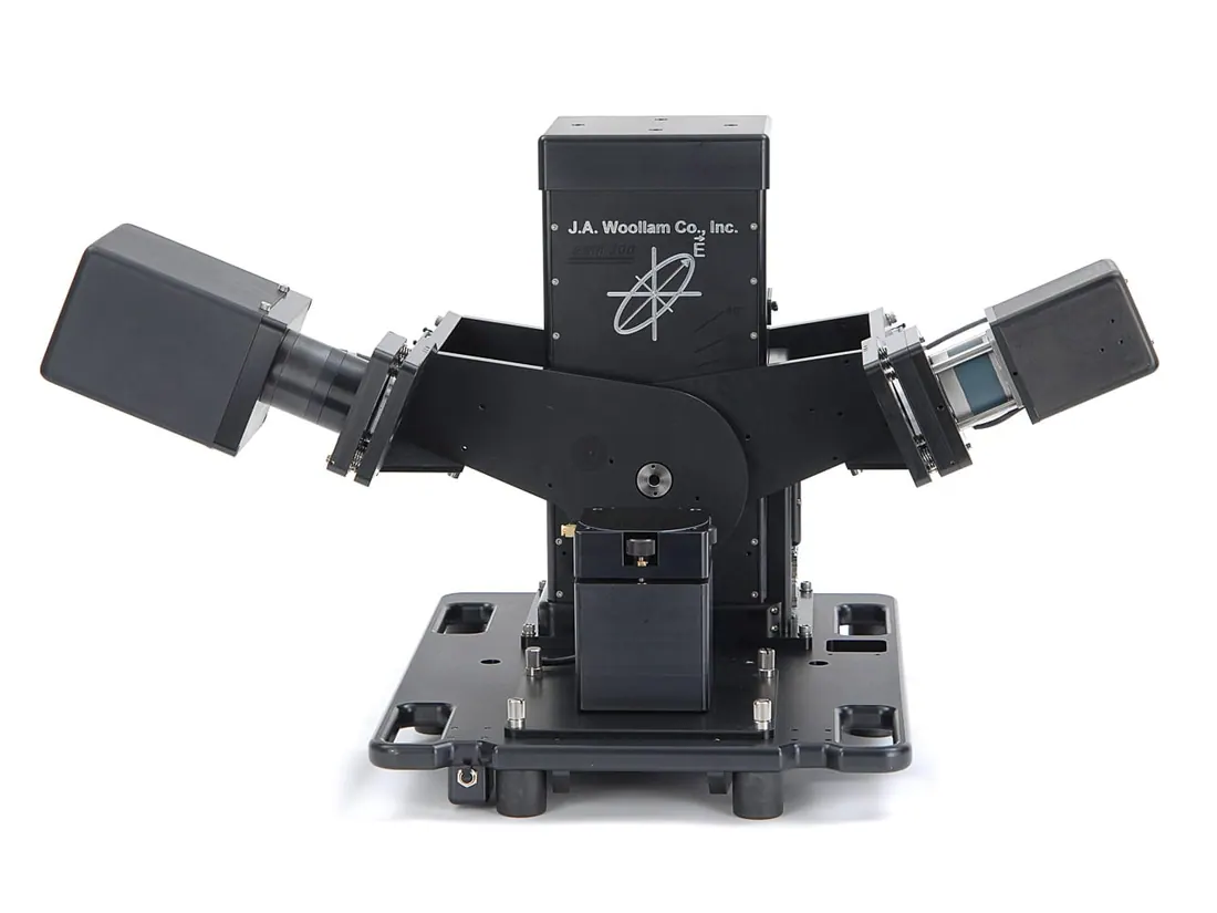
The M-2000 is a rotating compensator ellipsometer that collects hundreds of wavelengths at once with CCD detection. Modular optics let it sit on a table top base or attach to a process chamber, so the same instrument covers in situ monitoring, large area mapping and general thin film characterisation.
Technical Specifications
| Parameter | Value |
|---|---|
| Ellipsometer configuration | rotating compensator ellipsometer (RCE) |
| Spectral range | 193 to 1000 nm in the D configuration, NIR option adds 1005 to 1690 nm |
| Number of wavelengths | about 500 in the D configuration |
| Angles of incidence | 45 to 90 degrees automated angle base, 20 to 90 degrees vertical automated angle base |
| Data acquisition rate | 0.05 seconds minimum, 2 to 5 seconds typical for the complete spectrum |
| Maximum substrate thickness | 18 mm |
Get a Quote
Request an itemised quotation covering the proposed configuration, availability, lead time and agreed supply and support scope.
Useful details to share
- Materials, sample dimensions and process or measurement goal
- Required performance and existing instrument interfaces
Share what you know. You can start with your name and a phone number or email; final specifications can follow.
Not sure which configuration you need? Help me choose
Contact Vvon Technologies Limited about J.A. Woollam equipment requirements in Bangladesh.
Phone: +8801805987890 | Email: info@vvon.com.bd
More from Ellipsometry & Thin Film Metrology
- RC2 Ellipsometer
The RC2 uses two synchronously rotating compensators and was the first commercial spectroscopic ellipsometer to collect all 16 elements of the Mueller matrix. That makes it suited to anisotropic materials, liquid crystals and nanostructures as well as ordinary thin film work.
- theta-SE Ellipsometer
The theta-SE is a benchtop mapping ellipsometer for checking thin film uniformity across wafers up to 300 mm. A patented dual theta rotation stage, focused beam and camera alignment keep the footprint close to the wafer size while producing thickness and optical constant maps.
- VASE Ellipsometer
The VASE is the established variable angle research ellipsometer, using a rotating analyser with the AutoRetarder and a custom scanning monochromator. A vertical sample mount supports reflection, transmission and scattering geometries on semiconductors, dielectrics, polymers, metals and multilayers.