ACS200 Gen3 TE Automated Coater and Developer
Brand: SUSS MicroTec | Category: Nanotechnology
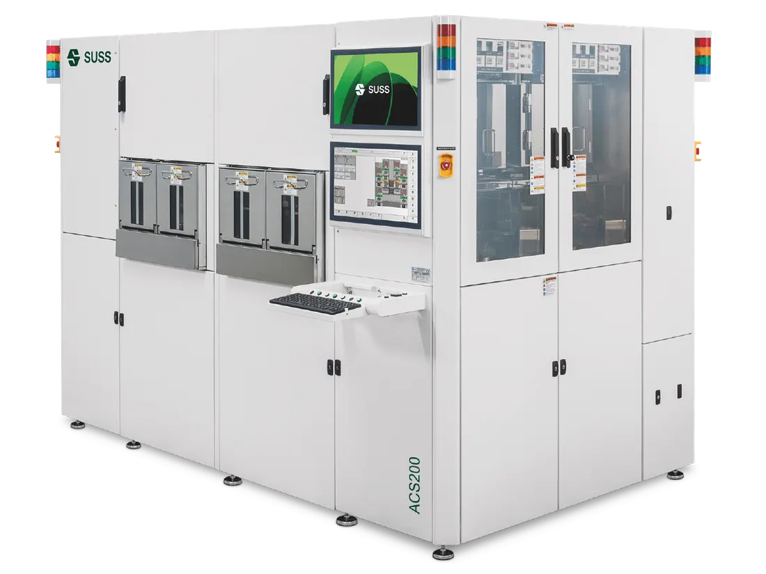
A throughput enhanced version of the ACS200 Gen3 cluster coater and developer for wafers from 100 mm to 200 mm. Up to six spinner modules can be fitted, and special tooling handles warped, ultra-thin and stacked wafers used in advanced packaging.
Technical Specifications
| Parameter | Value |
|---|---|
| Wafer sizes | 100 mm to 200 mm |
| Throughput | over 30% higher than ACS200 Gen3 |
| Spinner modules | up to six |
| Frame options | 3M, 5M and 6M |
| Resist viscosity | below 100 cp to below 20,000 cp |
| Film thickness | below 100 nm to below 250 µm |
Get a Quote
Request an itemised quotation covering the proposed configuration, availability, lead time and agreed supply and support scope.
Useful details to share
- Materials, sample dimensions and process or measurement goal
- Required performance and existing instrument interfaces
Share what you know. You can start with your name and a phone number or email; final specifications can follow.
Not sure which configuration you need? Help me choose
Contact Vvon Technologies Limited about SUSS MicroTec equipment requirements in Bangladesh.
Phone: +8801805987890 | Email: info@vvon.com.bd
More from Lithography & Patterning
- ASx Series Photomask Processing Platform
An automated photomask processing platform that carries out advanced bake, resist strip, clean and develop steps in one system. A 25 zone hotplate holds the bake temperature closely, which is what sets critical dimension uniformity on advanced masks.
- ACS200 Gen3 Automated Coater and Developer
An automated cluster coater and developer for wafers from 100 mm to 200 mm. Modular frames scale from research use up to high volume manufacturing, and the GYRSET closed cover method holds a solvent rich layer over the wafer for stable film thickness.
- MaskTrack Pro Series Photomask Cleaning Platform
A photomask cleaning and processing platform built for extreme ultraviolet lithography, 193i immersion work at 1x nm half-pitch and nanoimprint masks. The modular frame can be clustered with third party tools so storage, handling and processing stay in one controlled environment.