Alphacen 300 Drive
Brand: Nanosurf | Category: Nanotechnology
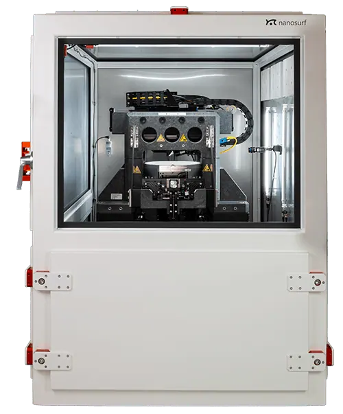
An AFM metrology system for 300 mm wafers, aimed at Angstrom level surface roughness and dimensional measurement in semiconductor quality control. WaveMode photothermal off-resonance imaging raises the line rate while holding tip sharpness, and wafer edge and sidewall inspection is supported.
Technical Specifications
| Parameter | Value |
|---|---|
| Scan range | 100 um x 100 um |
| Sample stage | programmable 300 mm x 300 mm |
| Wafer chucks | 300 mm and 200 mm |
| Line rate | up to 15 Hz with WaveMode, against 1 Hz standard |
| Positioning | sub-micron absolute accuracy |
| Automation | automatic wafer and cantilever alignment, KLARF file routines |
Get a Quote
Request an itemised quotation covering the proposed configuration, availability, lead time and agreed supply and support scope.
Useful details to share
- Materials, sample dimensions and process or measurement goal
- Required performance and existing instrument interfaces
Share what you know. You can start with your name and a phone number or email; final specifications can follow.
Not sure which configuration you need? Help me choose
Contact Vvon Technologies Limited about Nanosurf equipment requirements in Bangladesh.
Phone: +8801805987890 | Email: info@vvon.com.bd
More from Atomic Force & Scanning Probe Microscopy
- LensAFM
An AFM that mounts on the objective turret of an upright optical microscope or 3D profilometer, so a region found optically can be measured at nanometre resolution by rotating the turret. It returns 3D topography and can also map electrical, magnetic and mechanical properties.
- Alphacen 300 Flex
An industrial AFM built around the Flex-Mount tip-scanning head for samples that are too large or too heavy for a normal microscope. A dedicated acoustic enclosure cuts external noise, and extra translation or rotation axes can be added for awkward geometries.
- Nanite
One of the smallest AFM scan heads Nanosurf builds, made to be integrated into custom stages, production lines or existing setups. It measures sub-nanometre surface roughness on workpieces that cannot be cut down, including concave and curved surfaces.