DSC300 Gen3 Projection Scanner
Brand: SUSS MicroTec | Category: Nanotechnology
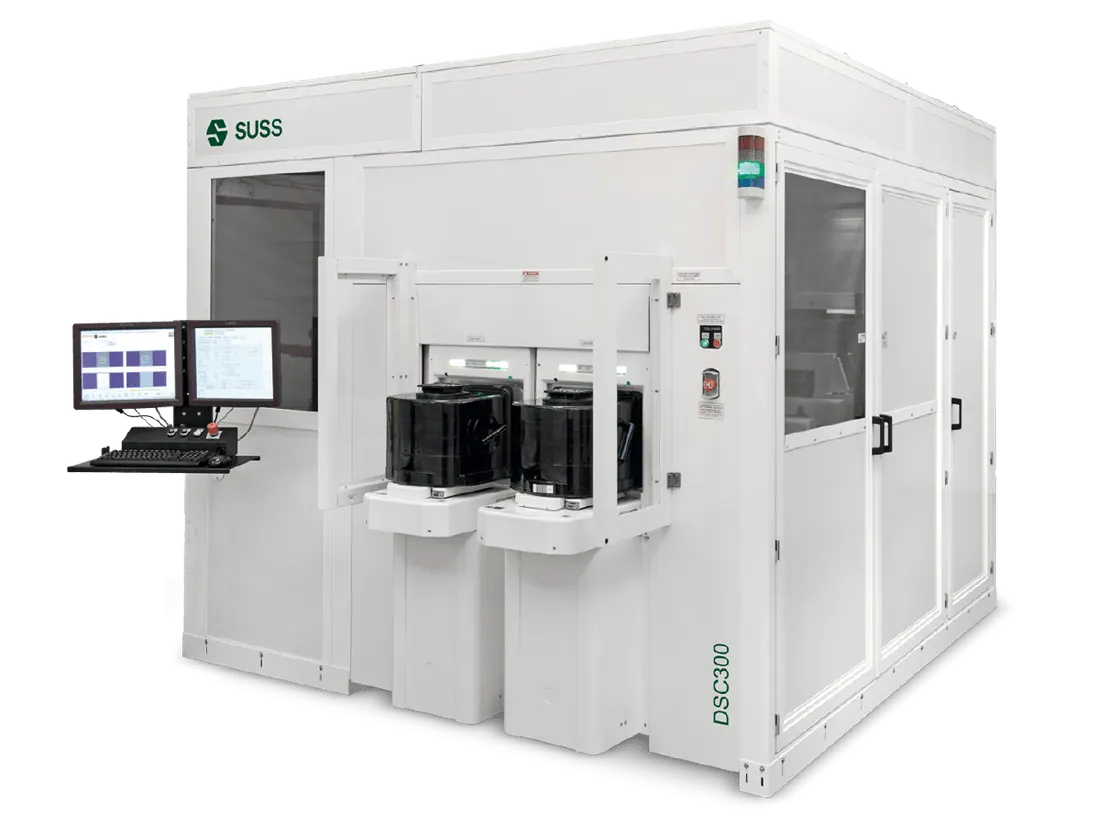
An automated projection lithography scanner for advanced packaging on 300 mm and 200 mm wafers. Wynne-Dyson optics print 2 µm lines and spaces with a large depth of focus, and the stitchless full field scan removes step field size limits on the layout.
Technical Specifications
| Parameter | Value |
|---|---|
| Wafer sizes | 300 mm, with 200 mm optional |
| Resolution | 2/2 µm lines and spaces |
| Overlay accuracy | 1.0 µm or better |
| Substrates | silicon, glass and silicon carbide |
| Warpage handling | up to 2 mm bow |
| Die shift compensation | ±200 ppm |
Get a Quote
Request an itemised quotation covering the proposed configuration, availability, lead time and agreed supply and support scope.
Useful details to share
- Materials, sample dimensions and process or measurement goal
- Required performance and existing instrument interfaces
Share what you know. You can start with your name and a phone number or email; final specifications can follow.
Not sure which configuration you need? Help me choose
Contact Vvon Technologies Limited about SUSS MicroTec equipment requirements in Bangladesh.
Phone: +8801805987890 | Email: info@vvon.com.bd
More from Lithography & Patterning
- LabSpin Series Spin Coater and Developer
A manual bench-top spin coater and developer for photolithography in laboratories. It spreads resist and other chemicals evenly over round or square substrates, and can be fitted with dispense, edge bead removal, puddle developer and nitrogen drying options.
- NIL-SFT8 Series Stamp Fabrication Tool
A table-top tool that makes working stamps for micro and nanoimprint lithography, sized to match the 8 inch MA/BA Gen4 mask aligners. UV-LED curing cuts stamp replication from hours to minutes for LED, MEMS, micro-optics and augmented reality applications.
- RCD8 Semi-Automated Coater and Developer
A semi-automated resist coating and developing module for wafers up to 200 mm. It suits research and small scale production, handling everything from very thin films to highly viscous thick resists, and runs alone or inside a SUSS LabCluster.