MA/BA Gen4 Series Mask and Bond Aligner
Brand: SUSS MicroTec | Category: Nanotechnology
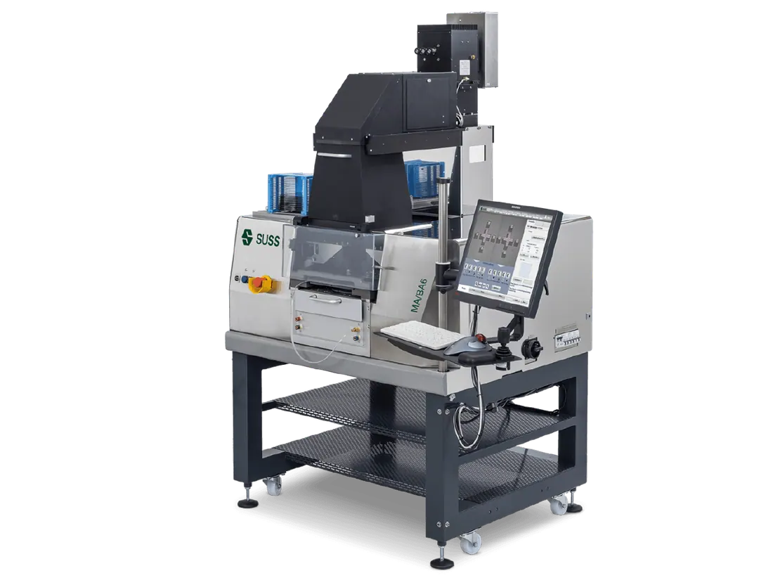
A semi-automated mask aligner and imprint platform for contact and proximity lithography. It exposes photoresist through a physical mask and also runs UV nanoimprint, serving MEMS and NEMS, advanced packaging, micro-optics and compound semiconductor work in research and pilot production.
Technical Specifications
| Parameter | Value |
|---|---|
| Overlay accuracy | 0.5 µm with optional DirectAlign technology |
| Resolution | down to 0.8 µm in hard, soft or vacuum contact |
| Alignment | top-side, bottom-side and infrared |
| Illumination | MO Exposure Optics with telecentric illumination |
| Versions | MA/BA6 Gen4, MA/BA8 Gen4 and MA/BA Gen4 Pro |
| Imprint | SMILE technology for standard to high-end imprint |
Get a Quote
Request an itemised quotation covering the proposed configuration, availability, lead time and agreed supply and support scope.
Useful details to share
- Materials, sample dimensions and process or measurement goal
- Required performance and existing instrument interfaces
Share what you know. You can start with your name and a phone number or email; final specifications can follow.
Not sure which configuration you need? Help me choose
Contact Vvon Technologies Limited about SUSS MicroTec equipment requirements in Bangladesh.
Phone: +8801805987890 | Email: info@vvon.com.bd
More from Lithography & Patterning
- MJB4 Manual Mask Aligner
A compact manual mask aligner for research and small volume production. It takes pieces from 5 by 5 mm up to 100 mm wafers, prints in soft, hard and vacuum contact, and also supports UV nanoimprint lithography on fragile materials.
- HMx Series Photomask Cleaning System
A compact manually loaded cleaning platform for photomasks and other delicate substrates, aimed at research and small series work. It brings develop, etch and cleaning steps into one cabinet, and also serves opto-electronics, OLED and semiconductor back end applications.
- MA300 Gen3 Mask Aligner
An automated mask aligner for 200 mm and 300 mm wafers in advanced packaging. It patterns through silicon vias, redistribution layers and bumping levels by proximity lithography, and copes with thick resist films that fall outside stepper capability.