MirrorCLEM System for Correlative Light and Electron Microscopy
Brand: Hitachi High-Tech | Category: Scientific & Laboratory Equipment
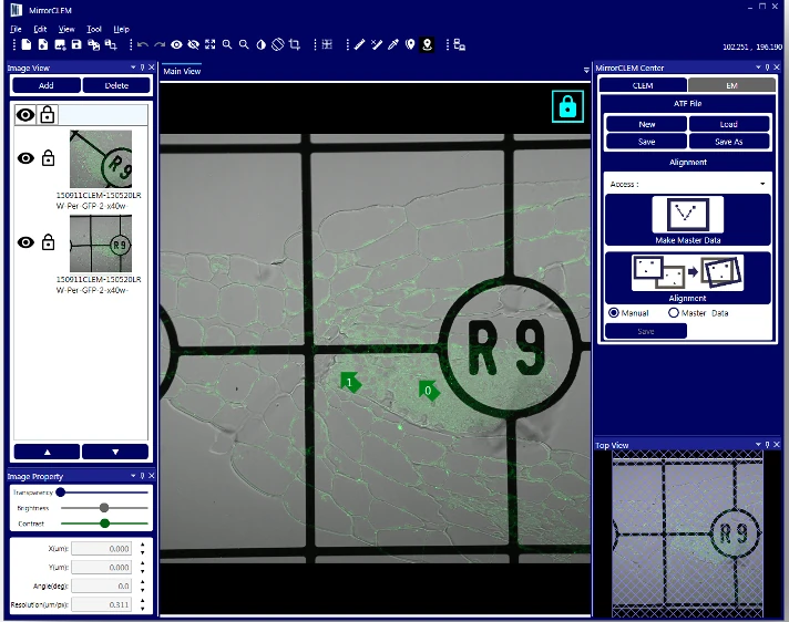
MirrorCLEM correlates specimens between optical and electron microscopes. A specimen imaged on any light microscope is transferred to the Hitachi SEM stage, where the optical image acts as an anchor map that drives the stage to a chosen region and overlays both images in real time.
Manufacturer-listed integration features
| Parameter | Value |
|---|---|
| Workflow | Correlative light and electron microscopy |
| Reference images | Optical and fluorescence microscopy images |
| SEM navigation | Region-of-interest positioning from the reference image |
| Image comparison | Live image overlay |
MirrorCLEM is a correlation and navigation system. Microscope resolution, image registration performance and compatible stages depend on the installed instruments and sample workflow. Checked 2026-09-29.
Confirm your configuration
Share the details you know so we can prepare a comparable, itemised offer.
- Specimen or clinical application and required imaging/measurement outputs
- Optics/source, detectors, working distance, stage and documentation options
- Room conditions, utilities, preparation accessories and operator training
Get a Quote
Request an itemised quotation covering the proposed configuration, availability, lead time and agreed supply and support scope.
Useful details to share
- Intended application, process or teaching activity
- Required capability and equipment it must work with
Share what you know. You can start with your name and a phone number or email; final specifications can follow.
Not sure which configuration you need? Help me choose
Contact Vvon Technologies Limited about Hitachi High-Tech equipment requirements in Bangladesh.
Phone: +8801805987890 | Email: info@vvon.com.bd
Back to Scientific & Laboratory Equipment
More from Electron Microscopy
- Tabletop Microscope TM4000PlusII/TM4000II
The TM4000II and TM4000PlusII are benchtop scanning electron microscopes for fast imaging with little sample preparation. They take specimens up to 80 mm across using backscattered electron detection, with secondary electron and mixed signal modes on the Plus model.
- Auto Capture for Array Tomography ACAT
ACAT is an automated image acquisition option for serial section analysis on Hitachi field emission SEMs. It aligns and captures a chosen region of interest across many consecutive sections, correcting for rotation, compression and tears so array tomography runs without operator input.
- Tabletop Microscope TM4000PlusIII/TM4000III
The TM4000III and TM4000PlusIII are the newest benchtop scanning electron microscopes in the Hitachi TM range. They image conductive and non conductive samples using a charge up reduction mode, and take specimens up to 80 mm diameter and 50 mm thick.