nanoANNEAL
Brand: Moorfield Nanotechnology | Category: Nanotechnology
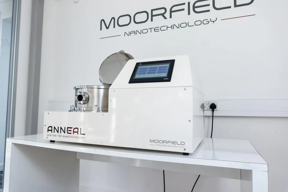
A benchtop thermal processing and annealing system for post deposition treatment. It is used for contact formation, crystallisation and interface work in photovoltaic, semiconductor and coatings research.
Technical Specifications
| Parameter | Value |
|---|---|
| System type | thermal processing and annealing |
| Process type | controlled thermal processing |
| Applications | photovoltaics, semiconductor materials, coatings and advanced materials research |
Get a Quote
Request an itemised quotation covering the proposed configuration, availability, lead time and agreed supply and support scope.
Useful details to share
- Materials, sample dimensions and process or measurement goal
- Required performance and existing instrument interfaces
Share what you know. You can start with your name and a phone number or email; final specifications can follow.
Not sure which configuration you need? Help me choose
Contact Vvon Technologies Limited about Moorfield Nanotechnology equipment requirements in Bangladesh.
Phone: +8801805987890 | Email: info@vvon.com.bd
More from Plasma Etching & Deposition
- Atomfab
Atomfab is a plasma enhanced atomic layer deposition system built for volume production of GaN power and RF devices. A remote plasma source designed for atomic scale processing gives low damage passivation and gate dielectric films, with clusterable automated wafer handling.
- nanoETCH
A compact plasma etching and surface modification system for low damage process development. It is used on 2D materials, graphene, silicon and oxide layers, and for substrate cleaning and surface activation before deposition.
- PlasmaPro ASP
PlasmaPro ASP is a remote plasma enhanced ALD system sharing the Atomfab platform. It deposits conformal oxides and nitrides across 200 mm wafers at high rate, using a low volume chamber for rapid gas exchange and a biased electrode for tuning film properties.