XBS300 W2W Hybrid Bonding Platform
Brand: SUSS MicroTec | Category: Nanotechnology
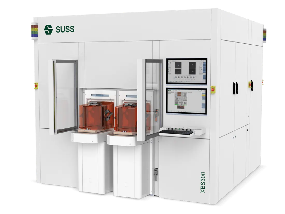
An automated hybrid bonding platform for wafer to wafer and collective die to wafer stacking on 200 mm and 300 mm wafers. Surface activation, metrology and bonding sit in one cluster for 3D stacked memory and 3D system on chip devices.
Technical Specifications
| Parameter | Value |
|---|---|
| Substrate sizes | 200 mm and 300 mm |
| Alignment accuracy | below 100 nm overlay |
| Thermal stability | ±25 mK over 12 hours with temperature control unit |
| Control | closed loop in X, Y and theta |
| Metrology | up to six modules in one cluster |
| Alignment technology | XBA with Inter Substrate Alignment |
Get a Quote
Request an itemised quotation covering the proposed configuration, availability, lead time and agreed supply and support scope.
Useful details to share
- Materials, sample dimensions and process or measurement goal
- Required performance and existing instrument interfaces
Share what you know. You can start with your name and a phone number or email; final specifications can follow.
Not sure which configuration you need? Help me choose
Contact Vvon Technologies Limited about SUSS MicroTec equipment requirements in Bangladesh.
Phone: +8801805987890 | Email: info@vvon.com.bd
More from Wafer Bonding
- XBC300 Gen2 SP Surface Preparation Cluster
A surface preparation cluster for hybrid bonding that cleans and activates wafers without an integrated bonder, so it can feed stand-alone bonding tools. It combines aqueous cleaning, vacuum plasma activation and in-line infrared void metrology.
- XBS200 Wafer Bonder
A fixture-less automated permanent bonder for wafer sizes up to 200 mm, aimed at volume production of MEMS, LED and 3D advanced packaging. Dropping mechanical fixtures gives flexible handling and lets spacing and vacuum conditions be logged digitally.
- XBC300 Gen2 D2W Wafer Bonder
An automated sequential die to wafer hybrid bonder that places and bonds individual dies onto a target wafer. Surface activation, die placement and metrology are integrated in one frame for high bandwidth memory and other 3D integrated circuit stacks.